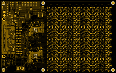
Physical access to electronics generally means all bets are off when it comes to information security. But in special cases this is just unacceptable and a better solution must be found. Consider the encryption keys used by point of sale machines. To protect them, the devices incorporate anti-tamper mechanisms that will wipe the keys from memory if the device is opened. One such technique is to use a mesh of traces on a circuit board that are monitored for any changes in resistance or capacitance. [Sebastian Götte] has been researching in this area and wrote a KiCad plugin to automatically generate tamper-detection mesh.
The idea is pretty simple, place traces very close to one another and it makes it impossible to drill into the case of a device without upsetting the apple cart. There are other uses as well, such as embedding them in adhesives that destroy the traces when pried apart. For [Sebastian’s] experiments he’s sticking with PCBs because of the ease of manufacture. His plugin lays down a footprint that has four pads to begin and end two loops in the mesh. The plugin looks for an outline to fence in the area, then uses a space filling curve to generate the path. This proof of concept works, but it sounds like there are some quirks that can crash KiCad. Consider taking a look at the code if you have the expertise to help make it more stable.
We’ve seen these anti-tamper meshes in practice in the VeriFone payment terminal that [Tom Nardi] tore down a couple of years ago. The approach that [Sabastian] took with the plugin actually produces a more complex mesh than was in use there as it only really used vertical lines for the traces.
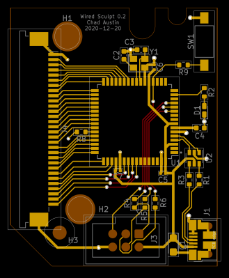
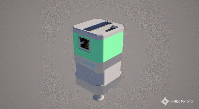
[chadaustin] has a favorite keyboard with a great ergonomic shape, key travel distance, and size, but after switching to Windows 10, the wireless connection introduced a terrible delay. Worse yet, the receiver is notoriously susceptible to interference from USB 3.0 hubs. To provide 128-bit AES encryption, the receiver is paired with the keyboard at the factory and cannot be replaced. If you lose that, you gain a highly ergonomic paper-weight. The solution for [chadaustin] was tethering the keyboard and receive several crash-courses in hardware hacking along the way. As evidenced by the responses to this project on ycombinator, many long-time fans of the Microsoft Sculpt Ergonomic Keyboard, introduced in 2013, suffer similar issues.
KiCad USB controller board layout
We really appreciate that [chadaustin] took an incremental approach, tackling one problem at a time and getting help from others along the way for first attempts at many complex steps. The proof-of-concept involved hand-soldering each lead from the keyboard matrix’s test pads to a QMK Proton C, which worked but couldn’t fit inside the keyboard’s case. For a more permanent and tidy solution, [chadaustin] tried a ribbon-cable breakout board and other microcontrollers, but none of those were compact enough to fit inside the case either. This required a custom PCB, another first for [chadaustin].
After a one-day intro to KiCad, [chadaustin] dug into the datasheets, completed a schematic for the board, and generously shared the process of choosing components and creating the layout. [chadaustin] ordered a board and found the mounting holes’ placement needed to be shifted.
With the full matrix mapped by [johnmilkspill], flashing QMK onto the AT90USB1286 controller went fairly smoothly. [chadaustin] chose to map both sides of the split spacebar back to the space key but did add a feature by repurposing the battery indicator LED to Caps Lock. And the results?
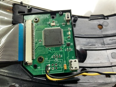
USB controller fits into the plastic case, wires added to ISP for bootloader button
According to testing done with Is It Snappy?, the latency dropped from the wireless 78 ms down to 65 ms over USB. More importantly, this latency is now consistent, unaffected by USB hubs, and there is no receiver to lose. Of course, [chadaustin] has ideas for future improvement, including regaining the multimedia function keys, as these kinds of hacks are never really done; they are just in the current revision. No word on the fate of the detached number pad, but that likely needs its own tether and is a project for another day.
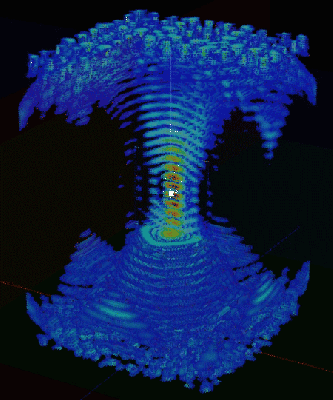
We are big fans of POV displays, particularly ones that move into 3D. To do so, they need to move even faster than their 2D cousins. [danfoisy] built a volumetric display that doesn’t move LEDs or any other digital display through space, or project light onto a moving surface. All that moves here is a bead of styrofoam and does so at up to 1 meter per second. Having low mass certainly helps when trying to hit the brakes, but we’re getting ahead of ourselves.
[danfoisy] and son built an acoustic levitator kit from [PhysicsGirl] which inspired the youngster’s science fair project on sound. See the video by [PhysicsGirl] for an explanation of levitation in a standing wave. [danfoisy] happened upon a paper in the Journal Nature about a volumetric display that expanded this one-dimensional standing wave into three dimensions. The paper described using a phased array of ultrasonic transducers, each with a 40 kHz waveform.
After reading the paper and determining how to recreate the experiment, [danfoisy] built a 2D simulation and then another in 3D to validate the approach. We are impressed with the level of physics and programming on display, and that the same code carried through to the build.
[danfoisy] didn’t stop with the simulations, designing and building control boards for each 100 x 100 grid of transducers. Each grid is driven by 2 Intel Cyclone FPGAs and all are fed 3D shapes by a Raspberry Pi Zero W. The volume of the display is 100 mm x 100 mm x 145mm and the positioning of the foam ball is accurate down to .01 mm though currently there is considerable distortion in the positioning.
Check out the video after the break to see the process of simulating, designing, and testing the display. There are a number of tips along the way, including how to test for the polarity of the transducers and the use of a Python script to place the grids of transducers and drivers in KiCad.
But wait, there’s more. There are 3 watt RGB LEDs at each upper corner of the display volume with PWM control to illuminate the foam ball, adding 7-bits of color information to each voxel. The original paper used this same phased array for haptic feedback and audible sound, but [danfoisy] says implementation of that right now just won’t fly. All the board files and code are on GitHub, so let us know where you take this next.
When we last checked in on the WiFiWart, an ambitious project to scratch-build a Linux powered penetration testing drop box small enough to be disguised as a standard phone charger, it was still in the early planning phases. In fact, the whole thing was little more than an idea. But we had a hunch that [Walker] was tenacious enough see the project through to reality, and now less than two months later, we’re happy to report that not only have the first prototype PCBs been assembled, but a community of like minded individuals is being built up around this exciting open source project.
Now before you get too excited, we should probably say that the prototypes didn’t actually work. Even worse, the precious Magic Smoke was released from the board’s Allwinner A33 ARM SoC when a pin only rated for 2.75 V was inadvertently fed 3.3 V. The culprit? Somehow [Walker] says he mistakenly ordered a 3.3 V regulator even though he had the appropriate 2.5 V model down in the Bill of Materials. A bummer to be sure, but that’s what prototypes are for.
Even though [Walker] wasn’t able to fire the board up, the fact that they even got produced shows just how much progress has been made in a relatively short amount of time. A lot of thought went into how the 1 GB DDR3 RAM would get connected to the A33, which includes a brief overview of how you do automatic trace length matching in KiCad. He’s also locked in component selections, such as the RTL8188CUS WiFi module, that were still being contemplated as of our last update.
Multiple boards make better use of vertical space.
Towards the end of the post, he even discusses the ultimate layout of the board, as the one he’s currently working on is just a functional prototype and would never actually fit inside of a phone charger. It sounds like the plan is to make use of the vertical real estate within the plastic enclosure of the charger, rather than trying to cram everything into a two dimensional design.
Want to get in on the fun, or just stay updated as [Walker] embarks on this epic journey? Perhaps you’d be interested in joining the recently formed Open Source Security Hardware Discord server he’s spun up. Whether you’ve got input on the design, or just want to hang out and watch the WiFiWart get developed, we’re sure he’d be happy to have you stop by.
The result is an interactive diagram that can be viewed in any web browser. Hovering over a pin or pad highlights those signals with a callout for the name, and clicking makes it stay highlighted for easier reference. Further information can be as detailed or as brief as needed.
Interestingly, Pinion isn’t a web service that relies on any kind of backend. The diagrams are static HTML and JavaScript only, easily included in web pages or embedded in GitHub documentation.
If you think Pinion looks a bit familiar, you’re probably remembering that we covered [Jan]’s much earlier PcbDraw tool, which turned KiCad board files into SVG renderings but had no ability to add labels or interactivity. Pinion is an evolution of that earlier idea, and its diagrams are able to act as both documentation and interactive reference, with no reliance on any kind of external service.
What do you get when you cross a day job as a Medical Histopathologist with an interest in 3D printing and programming? You get a fully-baked Open Source microscope, specifically the Portable Upgradeable Modular Affordable (or PUMA), that’s what. And this is no toy microscope. By combining a sprinkle of off-the-shelf electronics available from pretty much anywhere, a pound or two of filament, and a dash of high quality optical parts, PUMA cooks up quite possibly one of the best open source microscopy experiences we’ve ever tasted.
GitHub user [TadPath] works as a medical pathologist and clearly knows a thing or two about what makes a great instrument, so it is a genuine joy for us to see this tasty project laid out in such a complete fashion. Many a time we’ve looked into an high-profile project, only to find a pile of STL files and some hard to source special parts. But not here. This is deliberately designed to be buildable by practically anyone with access to a 3D printer and an eBay account.
The project is not currently certified for medical diagnostics use, but that is likely only a matter of money and time. The value for education and research (especially in developing nations) cannot really be overstated.
A small selection of the fixed and active aperture choices
The modularity allows a wide range of configurations from simple ambient light illumination, with a single objective, great for using out in the field without electricity, right up to a trinocular setup with TFT-based spatial light modulator enabling advanced methods such as Schlieren phase contrast (which allows visualisation of fluid flow inside a live cell, for example) and a heads-up display for making measurements from the sample. Add into the mix that PUMA is specifically designed to be quickly and easily broken down in the field, that helps busy researchers on the go, out in the sticks.
The GitHub repo has all the details you could need to build your own configuration and appropriate add-ons, everything from CAD files (FreeCAD source, so you can remix it to your heart’s content) and a detailed Bill-of-Materials for sourcing parts.
We covered fluorescence microscopy before, as well as many many other microscope related stories over the years, because quite simply, microscopes are a very important topic. Heck, this humble scribe has a binocular and a trinocular microscope on the bench next to him, and doesn’t even consider that unusual. If you’re hungry for an easily hackable, extendable and cost-effective scope, then this may be just the dish you were looking for.
KiCad has used the domain kicad-pcb.org since 2012 as the official source for information on and downloads of their popular open-source electronics design software. Unfortunately, the original domain name was purchased before KiCad was formalized as an organization, so it was not directly under their control. This all came to head when the old domain name was unexpectedly sold to an unnamed third party that was not affiliated with the project. Currently, the old domain is just a website covered in ads, but the KiCad team fears that it may be used maliciously in the future.
With KiCad’s popularity, thousands of tutorials, articles, and project guides over the years have included links to the old KiCad domain. A Google search in October 2021 found more than 19,000 instances of the old domain spread across the internet. [Seth_h] has called upon the community to make every effort possible to update old links, reducing the chance that people stumble across the wrong website.
[Editor’s Note: We think we got ’em all, let us know if we missed any.]
Luckily, Digikey has swooped in to help save the day. They purchased a new domain, kicad.org, from squatters and donated it to the KiCad Project. (Update: Digi-key donated the KiCad.org domain back in October of 2020 after noticing fishy squatters going back to at least 2016) [Seth_h] explains in his post that a number of safeguards have been put in place to prevent this from happening in the future, including not having the domain name owned by a single person, and having all KiCad trademarks registered to the Linux Foundation.
It’s widely accepted that the invention of the printing press by Gutenberg in the 15th Century was the event that essentially enabled the development of the modern world, allowing access to knowledge beyond anything that came before, even if the Chinese got in on the bookmaking act some 500 years previously. Fast-forward a few centuries more and we’ve got the ability to design electronics from our arm chairs, we can print 3D objects from a machine on the coffee table, and 3D modeling can be done by your kids on a tablet computer. What a time to be alive! So we think it’s perfectly fine that [Kris Slyka] has gone full circle and used all these tools to make printing plates for a small press, in order to produce cards for her Etsy business.
Now before you scoff, yes she admits quite quickly that KiCAD wasn’t the best choice for designing the images to print, since she needed to do a lot of post-processing in Inkscape, she could have just dropped the first step and started in Inkscape anyway. You live and learn. Once the desired image was fully vectorised, it was popped into OpenSCAD in order to extrude it into 3D, thickening the contact to the base to improve the strength a little.
[Kris] demonstrates using the registration marks to align the front and rear side plates, and even (mostly) manages adding a second colour infill for a bit more pizzazz. The results look a little bit wonky and imperfect, exactly what you want for something supposed to be handmade. We think it’s a nice result, even if designing it in KiCAD was a bit bonkers.
For those interested in the OpenSCAD code, have a butchers at this gist. This project is not the first 3D-printed printing press we’ve covered, checkout the Hi-Bred for an example, and here’s the Open Press Project if you’re still interested.
We like retro-computing and we like open source standards that allow easy project sharing. Vintage DEC computer enthusiast [Jay Logue] combines both of these in his recent project on GitHub, where he shares several KiCad templates for making your own Flip-Chip modules. Although named after the semiconductor packaging technique we are familiar with today, DEC Flip-Chips were introduced in 1964 as a modular electronics packaging system. These were used in many of DEC’s Programmable Data Processor (PDP) computers, beginning with the PDP-8 in 1965. DEC also had a Digital Laboratory Module family, which was a roll-your-own custom electronic system. The 1968 Digital Logic Handbook shows the available modules, and has the look and feel of the TTL Cookbook book which would come along six years later.
Flip-Chips came in a variety of sizes over the years: single-, double-, and quad-, and hex-height boards having standard- and extended-length. The PCB’s have 18 gold-plated fingers on one edge, later extended to 36 fingers double-sided, which plug into a backplane. Interconnections were typically wire-wrapped. A single height board is 127 x 62 mm (5 x 2-7/16 inches) with a labeled extractor bracket on one end. [Jay]’s repository has templates for five of the most popular variations, and making other sizes should be straightforward using these templates as a starting point.
While we pack a lot more functionality in similarly-sized circuit boards these days, many systems still use a modular design not unlike the Flip-Chips from over 50 years ago. Do you have any recollections of using Flip-Chips, or are you using them today? Let us know in the comments below.
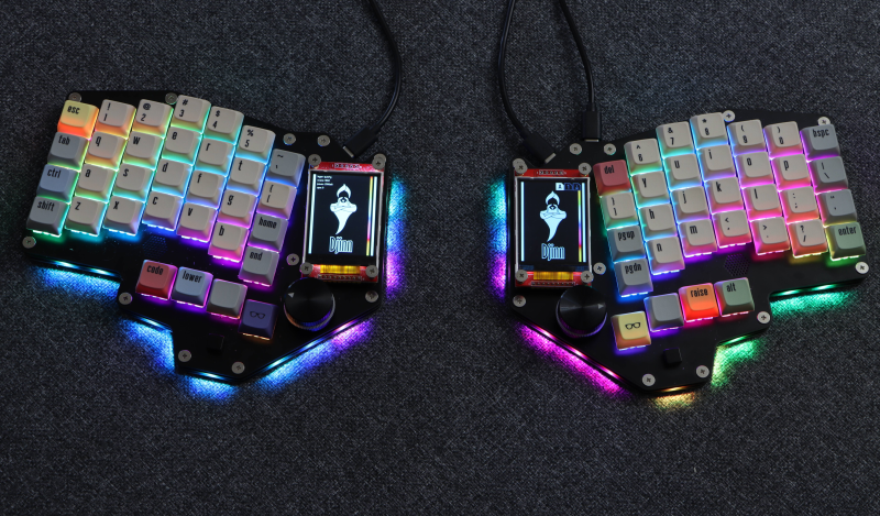
Sometimes a chance conversation leads you to discover something cool you’ve not seen before, and before you know it, you’re ordering parts for yet another hardware build. That’s what happened to this scribe the other day when chatting on some random discord, to QMK maintainer [Nick Brassel aka tzarc] about Djinn, a gorgeous 64-key split mechanical keyboard testbed. It’s a testbed because it uses the newest STM32G4x microcontroller family, and QMK currently does not have support for this in the mainline release. For the time being, [Nick] maintains a custom release, until it gets merged.
Hardware-wise, the design is fabulous, with a lot of attention to detail. We have individual per-key RGB LEDs, RGB underglow, a rotary encoder, a five-way tactile thumb switch, and a 240×320 LCD per half. The keyboard is based on a three PCB stack, two of which are there purely for structure. This slick design has enough features to keep a fair few of us happy.
Interestingly, when you look at the design files (KiCAD, naturally) [Nick] has chosen to take a mirrored approach to the PCB. That means the left and right sides are actually the same PCB layout. The components are populated on different sides of the PCB depending on which half you’re looking at! By mirroring footprints on both PCB sides, and hooking everything up in parallel, it’s possible to do it all with a single master layout.
This is a simple but genius idea that this scribe hadn’t come across before (the shame!) Secondarily it keeps costs down, as your typical Chinese prototyping house will not deal in PCB quantities below five, so you can make two complete keyboards on one order, rather than needing two orders to make five. (Yes, there are actually three unique PCBs, but we’re simplifying the situation, ok?)
Now, if only this pesky electronics shortage could abate a bit, and we could get the parts to build this beauty!
When it comes to electronic design, breadboarding a circuit is the fun part — the creative juices flow, parts come and go, jumpers build into a tangled mess, but it’s all worth it when the circuit finally comes to life. Then comes the “What have I done?” phase, where you’ve got to backtrack through the circuit to document exactly how you built it. If only there was a better way.
Thanks to [Nick Bild], there is, in the form of the “Schematic-o-matic”, which aims to automate the breadboard documentation process. The trick is using a breadboard where each bus bar is connected to an IO pin on an Arduino Due. A program runs through each point on the breadboard, running a continuity test to see if there’s a jumper connecting them. A Python program then uses the connection list, along with some basic information about where components are plugged into the board, to generate a KiCad schematic.
[Nick] admits the schematics are crude at this point, and that it’s a bit inconvenient to remove some components, like ICs, from the breadboard first to prevent false readings. But this seems like one of those things where getting 80% of the work done automatically and worrying about the rest later is a big win. Plus, we can see a path forward to automatic IC probing, and even measurement of passive components too. But even as it is, it’s a great tool.
There are many, many video tutorials about designing the functional side of PCBs, giving you tips on schematic construction, and layout tips. What is a little harder to find are tutorials on the graphical aspects, covering the process from creating artworks and how you can drive the tools to get them looking good on a PCB, leveraging the silkscreen, solder and copper layers to maximum effect. [Stuart Patterson] presents his guide for Advanced PCB Graphics in KiCAD 6.0 and Inkscape, (Video, embedded below) to help you on your way to that cool looking PCB build.
Silkscreen layers in yellow, solder mask opening in red
The first step is to get your bitmap, whether you create it yourself, or download it, and trace it into a set of vectors using the Inkscape ‘trace bitmap’ tool. If you started with an SVG or similar vector shape, then you can skip that stage.
Next simply create a PCB outline shape by deleting all the details that aren’t part of the outline. A little scaling here and there to get the dimensions correct and you’re done with the first part. [Stuart] has an earlier video showing that process.
The usability improvements in KiCAD 6.0 are many, but one greatly demanded feature is the ability to group objects, just like you do in Inkscape and any other vector graphics tool for that matter. That means you can simply import that SVG outline into the Edge.Cuts PCB layer and all the curves will be nicely tied together. Next you select the details you want for the silkscreen layer, solder mask removal layers and any non-circuit copper. In Inkscape it would be wise to use the layers feature to assign the different material types to a uniquely named layer, so they can be hidden for exporting. This allows you to handle silk, mask and copper PNG exports from a single master file, in addition to any vector details for outline, slots and holes.
Once you have PNG bitmap exports for the silk, mask etc. you need to create a footprint inside a board-specific library, using the KiCAD image converter tool. It was interesting to note that you can export a new image footprint from the tool and paste it straight into the footprint editor, and tweak all the visibility details at the same time. That will save some time and effort for sure. Anyway, we hope this little tutorial from [Stuart] helps, and we will be sure to bring you plenty more in the coming months.
I’ve been following the development of KiCAD for a number of years now, and using it as my main electronics CAD package daily for a the last six years or thereabouts, so the release of KiCAD 6.0 is quite exciting to an electronics nerd like me. The release date had been pushed out a bit, as this is such a huge update, and has taken a little longer than anticipated. But, it was finally tagged and pushed out to distribution on Christmas day, with some much deserved fanfare in the usual places.
So now is a good time to look at which features are new in KiCAD 6.0 — actually 6.0.1 is the current release at time of writing due to some bugfixes — and which features originally planned for 6.0 are now being postponed to the 7.0 roadmap and beyond.
Changes
As is often the case with big updates, most of the largest changes are invisible to the user, and are the result of significant code refactoring in order to create consistent frameworks for the developers to work to, whilst they add new features from the wish list. What we as users see are the changes that this under-the-hood work enables. A feature change often seems ‘easy’ from a user perspective, but requires extensive internal changes and a lot of developer effort behind the scenes. KiCAD is an old project, with three decades of code history, so unpicking a lot of that to build these consistent frameworks for future work has been a monumental undertaking. In a recent Contextual Electronics podcast interview with KiCAD developer [John Evans] the burden of this code history was explained in this context in a very helpful way, and you can really get a feel for just how tricky it can be to navigate as a new developer and why this update is so important.
Libraries and Schematic Files
Following on from the S-expression PCB library format KiCAD 5.0 introduced, symbol libraries are now described in the same format. KiCAD 6.0 will make the migration at the touch of a button. This format is designed to be human readable, which in turn makes it much easier to write other software that creates or modifies these files.
One useful change is that the dependency upon schematic libraries has been dropped, so once a sheet is completed, you only need the sheet file to open it. No more broken schematic sheets! No more chasing libraries for a handful of symbols, and design reuse is vastly simplified.
These changes, of course, have a downside — once you have opened and migrated a project from KiCAD 5.x, there is no way to go back, so make sure you make a copy first and/or use revision control. That said, so far, I have had no issues that would force me to move back to the previous release.
New Features
Curvy hashed goodness. In all seriousness, this is great news for flex PCB design
The updated or new feature list is so extensive, that simply listing it all here would be quite a long undertaking. As luck would have it, I don’t need to, as [Peter Dalmaris] published a preview of the changes coming in version 6.0 at the start of the year, when most new features and changes were already rolled out into the ‘nightlies’ for beta testing. The first highlight for me is the big update to the Design Rules Checking (DRC) system, which is now significantly more powerful and configurable, and even allows custom rules per board. This feature has its own special specification syntax, and will take some time to learn, but looks like time well spent. Another greatly improved area is the visibility control side panel, easing control of visible elements and helping produce a clutter-free display as you work between layers.
Curved traces look great. Feel free to argue in the comments about their utility. (Maybe in microwave RF designs?) Hashed zone fills are great for those of us designing flexible circuits, or planes that need to be copper-light for thermal reasons. And while we’re talking about zone fills, there is now a configuration option to allow filleting of corners outside of the zone outline, which makes filleted zones look a lot nicer.
One feature that probably isn’t new to KiCAD 6.0, but I hadn’t noticed before, concerns drag selections. When click-dragging around a bunch of objects, to make a grouped selection, it turns out the tool is direction-sensitive. Dragging from left-to-right only selects items that are completely contained within the box — but the opposite — selecting from right-to-left selects any items the box touches, even partially. I really wish I’d have found this out years ago! Thanks to [Stargirl @thevalkyrie] on Twitter for the heads up on that.
Other big improvements are the unified project setup, with many more options to set PCB properties like stack-up, and at long last, net class definitions at schematic level with customisable colours and styles to improve clarity of design intention. Lastly, there is a new ‘rules file’ import feature for PCB fab definitions and constraints, which will hopefully enable easier setup of board constraints when moving between different manufacturer processes, and reduce the likelihood of the annoying issue of designing a tight board to the wrong rule set. (Never done that myself, oh no.)
The PCB editor has so many updates and design improvements that there is not the space here to do it justice. I suggest reading the release notes instead! The short version is that the workflow has been streamlined, tools have been expanded and regrouped and made more visible, and some of KiCAD’s rough edges and other oddities have been smoothed over.
A New Plugin And Content Manager
One very nice feature that has snuck in to release 6.0 at the last minute is the first version of the new plugin and content manager. This vastly improves the user experience for adding plugins, with the KiCAD project maintaining its own online repository, and new plugins arriving all the time.
This integrated management will enable much better visibility of community-contributed themes, libraries and software extensions, and will surely mark a new era of KiCAD customisation. At the time of writing, notable plugins include the excellent InteractiveHtmlBom, which I use extensively, KiBuzzard for your fancy labelling needs, and KiKit for panelisation tasks.
The repository is in the early stages, but new component libraries are already popping up there too. It’s isn’t entirely push button, however. If a Python plugin is complex enough to depend up non-default installed modules, then you need to manually invoke the Python package manger pip to meet those dependencies. Luckily, at least on windows, there is a special command interpreter menu item with all the Python paths set correctly, so it is a trivial matter to pop open a terminal, invoke pip, then crack on with your project. The Python plugins that need manual intervention should prompt you with instructions when they are first installed. Hopefully future versions of the package manager will deal with such issues automatically! Finally, in true open source style, it is easy enough to add additional repositories, so you can disconnect yourself from the official version if you or your organisation has other needs.
Postponed to 7.0
The wish list for KiCAD 6.0 was really big and ambitious, and in order to get something worth using out quicker, a feature freeze was enacted early last year in order to finish off the features that made the cut and iron out the bugs. Many really good features didn’t make enough progress, or relied on other changes before work could start. Regardless, let’s look at a few of the planned new tricks for the next release.
First off, the Python API is going to change. API access to the schematic object is currently not supported, making it impossible to create plugins that manipulate schematics. This will change in release 7.0, but not until the underlying schematic object is refactored to enable it. There is a planned object properties/introspection API which allow a new class of plugins to be created for even more powerful design manipulation. Fingers crossed!
The next big feature again concerns the schematic editor. Orthogonal wire dragging will be implemented, to enable moving symbols around and keeping the connections looking good. Net-ties! We’re going to finally get proper net-tie support!
The PCB editor is planned to get teardrop support, as well as modern features like trace refining. The ability to adjust trace length matching/meandering is also planned. Design reuse will be boosted by support for layout snippets, and there will be better support for pad stacks and more powerful thermal relief control.
The final and most interesting future feature — for me at least — is the planned PCB constraints management system. This is intended to allow constraints to be specified in the schematic and passed into the board editor, in order to constrain placement and layout as well as feed into the DRC system. This will be an epic feature if it actually happens. Details are scarce right now, but rest assured I’ll be tracking it.
So there we have it, a brief overview of where we are and where we’re going in the world of KiCAD. Keep an eye out for future stories and guides about this fantastic tool, as the KiCAD future is bright, and it’s all open source and therefore free from licensing charges.
Need some help finally taking the plunge to move to KiCAD? Then you’re going to want to checkout the official KiCAD forum, and drop in to the super active KiCAD Discord from time to time.
Let’s make one thing abundantly clear. We do not, under any circumstances, recommend you replace your existing collection of wrenches with ones made out of PCBs. However, as creator [Ben Nyx] explains, they do make for an extremely cheap and lightweight temporary tool that would be perfect for distributing with DIY kits.
This clever open hardware project was spawned by [Ben]’s desire to pack an M3 wrench in with the kits for an ESP32-based kiln controller he’s developing. He was able to find dirt cheap screwdrivers from the usual import sites, but nobody seemed to stock a similarly affordable wrench. He experimented with 3D printing them, but in the end, found the plastic just wasn’t up to the task. Then he wondered how well a tiny wrench cut from a PCB would fare.
The answer, somewhat surprisingly, is pretty well. We wouldn’t advise you try to crank your lug nuts down with one, but for snugging up a couple nuts that hold down a control board, they work a treat. [Ben] came up with a panelized design in KiCad that allows 18 of the little wrenches to get packed into a 100 x 100 mm PCB suitable for production from popular online board houses. Manufactured from standard 1.6 mm FR4, they come out to approximately 10 cents a pop.
Since [Ben] has been kind enough to release his design under the MIT license, you’re free to spin up some of these wrenches either for your own kits or just to toss in the tool bag for emergencies. We’d love to see somebody adapt the design for additional sizes of nuts, or maybe figure out some way to nest them to sneak out a couple extra wrenches per board.
First hand-built prototype. Nurse! isopropyl alcohol, stat!
Prolific hacker [Sulfuroid] is a medical doctor by day, and an electronics hobbyist by night, and quite how he finds the time, we have no idea.
The project we want to highlight is an ESP32 based LED smart watch, which we’ll sure you’ll agree, looks pretty nicely developed so far, and [Sulfuroid] has bigger plans, as you may find, when you dig into the GitHub repo. This analog-style design uses four groups of 0603-sized LEDs, arranged circularly to indicate the passage of time, or anything else you fancy. Since there are four control buttons, a pancake vibration motor, as well as Wi-Fi and Bluetooth, the possibilities are endless.
In order to stand a hope of driving those 192 LEDs from a single ESP32-Pico-D4, it was necessary to use a multiplexed LED driver, courtesy of the Lumissil IS31FL3733 device, which can handle arrays up to 12 x 16 devices. This chip is one to remember, since it has some really nice features, such as global current control to reduce CPU overhead, automatic breathing loops for those fancy fade effects, and even includes a handy open/short detection function, so it can report back assembly problems, assisting in reworking your dodgy soldering!
Routing circular arrays is such a pain.
Power and interfacing are taken care of via USB-C, with a TP4054 single Li-Ion cell charger chip handling the battery. This is a Taiwanese clone of the popular LTC4054, but that chip may be a bit hard to get at the moment. There is the common-as-muck CP2104 USB chip dealing with the emulated serial port side of things, since for some reason, the ESP32 still does not support USB. The Pico-D4 does have RTC support, but [Sulfuroid] decided to use a DS3231M RTC chip instead. We noticed the touch functionality wasn’t broken out – that could be added easily in the next revision!
Robotic mowers are becoming a common sight in some places, enabled by the cost of motors and the needed control electronics being much lower, thanks to the pace of modern engineering. But, in many cases, they still appear to be really rather dumb, little more than a jacked up bump-and-go with a spinning blade. [Clemens Elflein] has taken a cheap, dumb mower and given it a brain transplant based around a Raspberry Pi 4 paired up with a Raspberry Pi Pico for the real time control side of things. [Clemens] is calling this OpenMower, with the motivation to create an open source robot mower controller with support for GPS navigation, using RTK for extra precision.
The donor robot was a YardForce Classic 500, and after inspection of the control PCB, it looks like many other robot mower models are likely to use the same controller and thus be compatible with the openmower platform. A custom mainboard houses the Pi 4 and Pico, an ArduSimple RTK GPS module (giving a reported navigational accuracy of 1 cm,) as well as three BLDC motor drivers for the wheels and rotor. Everything is based on modules, plugging into the mainboard, reducing the complexity of the project significantly. For a cheap mower platform, the Yardforce unit has a good build quality, with connectors everywhere, making OpenMower a plug and play solution. Even the user interface on top of the mower was usable, with a custom PCB below presenting some push buttons at the appropriate positions.
OpenMower mainboard
Motor control is courtesy of the xESC project, which provides FOC motor control for low cost, interfacing with the host controller via a serial link. This is worth looking into in its own right! On the software side of things, [Clemens] is using ROS, which implements the low level robot control, path planning (using code taken from Slic3r) as well a kinematics constraints for object avoidance. The video below, shows how simple the machine is to operate — just drive it around the perimeter of lawn with a handheld controller, and show it where obstacles such as trees are, and then set it going. The mower is even capable of mowing multiple lawns, making the journey between them automatically!
The first PCBs we built involved a draftsman laying out large pieces of tape. The finished artwork would be photographically reduced to produce the board. This solved a few problems. It was easier to work on the large pieces and any errors were reduced by the scale amount. Boards from this era have a distinct appearance because the tracks are generally curved. But when computer-aided drafting took over, the early packages couldn’t deal with wavy lines making all sorts of angles. So traces started appearing at very common angles like 45 degrees or 90 degrees only. If you use KiCAD, though, there’s no reason to have rectilinear traces. Now there is a plugin to help make your boards appear like old-fashioned circuit boards.
The video by [mitxela] below talks about how we got here and debunks some common myths about PCB design. The plugin produces rounded corners and teardrop-shaped pads. There’s also a second post on the topic with more details. The effect isn’t just ornamental. There are some reasons graceful traces might be better than sharp angles.
What would a HAL9000 look like if it eye were yellow and sat atop a front panel inspired by an Altair 8800? You’d have today’s feature, [Stephan]’s BerlinUhr, a gorgeous little take on a Berlin Clock.
At Hackaday, we have a soft spot for clock builds. They’ve graced our pages from early times. When we saw this ultra cool Berlin Clock, we couldn’t resist the urge to share it with all of our readers. For those of you not familiar with a Berlin Clock, it’s a clock that consists of 24 lights, and was the first of its kind back in 1975.
[Stephan]’s build is notable because not only is it a beautiful design, but the work that went into the design and build. At several inches tall, the BerlinUhr is supported solely by a USB-C connection, although it can also be hung on a wall. The RTC is backed up by a CR1216, and an ATtiny167 provides the brains for the operation.
A neat part of the build comes with the KPS-3227 light sensor, used to adjust the LED brightness according to ambient lighting. Rather than being a straightforward part to insert into the PCB, KiCad’s footprint had some pins reversed, causing [Stephan] to learn how to correct it and contribute the fix to KiCad. Well done!
[Neumi] over on Hackaday.IO wanted a simple-to-use way to drive stepper motors, which could be quickly deployed in a wide variety of applications yet to be determined. The solution is named Ethersweep, and is a small PCB stack that sits on the rear of the common NEMA17-format stepper motor. The only physical connectivity, beside the motor, are ethernet and a power supply via the user friendly XT30 connector. The system can be closed loop, with both an end-stop input as well as an on-board AMS AS5600 magnetic rotary encoder (which senses the rotating magnetic field on the rear side of the motor assembly – clever!) giving the necessary feedback. Leveraging the Trinamic TMC2208 stepper motor driver gives Ethersweep silky smooth and quiet motor control, which could be very important for some applications. A rear-facing OLED display shows some useful debug information as well as the all important IP address that was assigned to the unit.
Control is performed with the ubiquitous ATMega328 microcontroller, with the Arduino software stack deployed, making uploading firmware a breeze. To that end, a USB port is also provided, hooked up to the uC with the cheap CP2102 USB bridge chip as per most Arduino-like designs. The thing that makes this build a little unusual is the ethernet port. The hardware side of things is taken care of with the Wiznet W5500 ethernet chip, which implements the MAC and PHY in a single device, needing only a few passives and a magjack to operate. The chip also handles the whole TCP/IP stack internally, so only needs an external SPI interface to talk to the host device.
Talking about firmware for a moment, to ease deployment, the network configuration is handled by DHCP, although some control over MAC address assignment is promised for the future. All control is via UDP over ethernet, and again the basic functionality is there, but some niceties such as motor synchronisation and state querying are again subject to further releases. Hardware design is implemented in KiCAD and FreeCAD, with Arduino covering the firmware and host control side in python. You can read all about it on the Ethersweep project GitHub, what is there not to like?
If you thought you’d seen this stepper-mounted driver setup before, you’d be correct, here’s a Hackaday Prize 2017 Entry for a CANBUS controlled driver. We also saw this on Dummy: the obscenely well made robot arm by [Zhihui Jun], which if you missed it, then do circle back and take a look, you won’t regret it!
A team from the Institute for Automation of Complex Power System (ACS) at RWTH Aachen University have been working for a while on the analysis of widely distributed power systems. In a drive to move away from highly specialised (and expensive) electronics platforms, they have produced some instrumentation designed to operate with the Raspberry Pi platform, and an open source software stack. They call the platform the SMU (Synchronised Measurement Unit.) The SMU consists of a HAT sitting on an RPi3, inside a 3D printed box that is intended to attach to a DIN rail. After all, this is supposed to be an industrial platform.
Hardware wise, the star of the show is the Texas Instruments ADS8588S which is a 16-bit 8-channel simultaneous sampling ADC. This is quite a nice device, with 200 kSPS throughput and a per-channel programmable front end, packaged in a hacker-friendly 64-pin QFP. What makes this project interesting however, is how they solved the problem of controlling the sampled data acquisition and synchronisation.
1-PPS and BUSY edges converted to levels, then OR’d to trigger the DMA
By programming the ADC into byte-parallel mode, then using the BCM2837 Secondary Memory Interface (SMI) block together with the DMA, samples are transferred into memory with minimal CPU overhead. An onboard U-Blox Max-M8 GNSS module provides a 1PPS (top of second pulse) signal, which is combined with the ADC busy signal in a very simple manner, enabling both sample rate control as well as synchronisation between multiple units spread out in an installation. They reckon they can get synchronisation to within 180 ns of top-of-second, which for measuring relatively slow-changing power systems, should be enough. The HAT PCB was created in KiCAD and can be found in the SMU GitHub hardware section, making it easy to modify to your needs, or at least adjust the design to match the parts you can actually get your hands on.
Software-wise, the full stack is provided from the kernel module that deals with the low-level stuff, offering up /dev/SMU, right up to the management daemon and a QT-based GUI. A full system level description can be found on the associated Open Access article.
We see many power monitor projects on Hackaday, since a little more knowledge of power usage can save you in the long run. Here’s another RPi HAT project, for just this purpose. Of course, you don’t have to be this clever, if you have an appropriate electricity meter, you could just count blinks and call it a day.

 The idea is pretty simple, place traces very close to one another and it makes it impossible to drill into the case of a device without upsetting the apple cart. There are other uses as well, such as embedding them in adhesives that destroy the traces when pried apart. For [Sebastian’s] experiments he’s sticking with PCBs because of the ease of manufacture. His plugin lays down a footprint that has four pads to begin and end two loops in the mesh. The plugin looks for an outline to fence in the area, then uses a space filling curve to generate the path. This proof of concept works, but it sounds like there are some quirks that can crash KiCad. Consider taking a look at the code if you have the expertise to help make it more stable.


 making uploading firmware a breeze. To that end, a USB port is also provided, hooked up to the uC with the cheap CP2102 USB bridge chip as per most Arduino-like designs. The thing that makes this build a little unusual is the ethernet port. The hardware side of things is taken care of with the
