The last two years has been a particularly exciting time for KiCad, for users, casual contributors, and for the core developers too. Even so, there are many cool new features that are still in process. One bottleneck with open-source development of complex tools like KiCad is the limited amount of time that developers can devote for the project. Action plugins stand to both reduce developer load and increase the pace of development by making it easier to add your own functionality to the already extensible tool.
Sometime around version 4.0.7 (correct us if we’re wrong), it was decided to introduce “action plugins” for KiCad, with the intention that the larger community of contributors can add features that were not on the immediate road map or the core developers were not working on. The plugin system is a framework for extending the capabilities of KiCad using shared libraries. If you’re interested in creating action plugins, check out documentation at KiCad Plugin System and Python Plugin Development for Pcbnew. Then head over to this forum post for a roundup of Tutorials on python scripting in pcbnew, and figure out how to Register a python plugin inside pcbnew Tools menu.
Since version 5.0, we’ve seen an explosion of extremely useful action plugins for KiCad that have added some very useful bells and whistles. The KiCad website lists a couple of external tools, but there’s a lot of action happening out there, so we decided to round up some of the more useful ones.
KiCad StepUp Tools
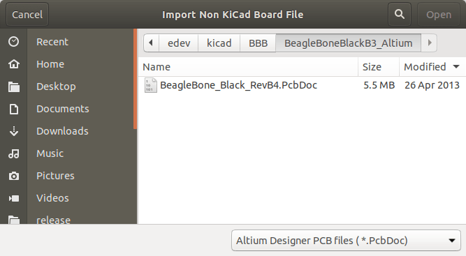
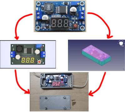
Action Plugins came about as a result of work done earlier to improve the KiCad 3D model viewer by adding support for other CAD formats besides VRML. This resulted in the ability to use STEP formats for component models in KiCad 3D viewer, and the STEP export feature for the complete board. If you need nice looking renders, VRML format suits well. But if you want to import to CAD, then STEP format works better. Based on this, one early feature add-on wasn’t really an action plugin, but a workbench for FreeCAD which created a bridge between KiCad and FreeCAD. [Maurice]’s StepUp Tools offers integration between EDA KiCad and Mech FreeCAD. There’s an active thread discussing KiCad StepUp Tools on the forum with lots of demo videos and helpful assistance.
RF Tools for KiCad
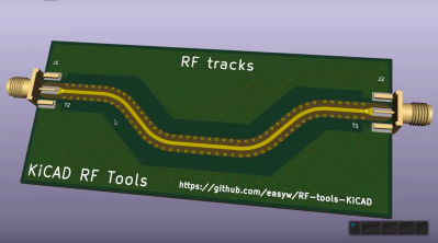
![]() Recently, [Maurice] has released RF Tools for KiCad which include a collection of plugin’s that address a long felt need for RF design. The suite includes footprint wizards for designing mitred bends, tapered track connectors, and arc tracks (radius bends) for RF layout. These tools work by creating footprints, so it isn’t perfect, but it’s a big step in the right direction.
Recently, [Maurice] has released RF Tools for KiCad which include a collection of plugin’s that address a long felt need for RF design. The suite includes footprint wizards for designing mitred bends, tapered track connectors, and arc tracks (radius bends) for RF layout. These tools work by creating footprints, so it isn’t perfect, but it’s a big step in the right direction.
Also included is a set of action plugins for arc track corners, track length measurement, and a mask expansion tool. The expansion tool lets you adjust mask clearances for tracks and is handy for RF layout and for high current applications where you want to layer up extra solder on top of exposed copper tracks. It may also appeal to the artistic folks who want more control over track layout and visual design. Rounded tracks will also be pretty handy when designing flex PCBs. It’s worth pointing out that the arc action plugin will create segmented arcs while the arc footprint wizard will produce a smooth arc, so both have their pros and cons. If you get stuck, there’s an active thread on the forum for help and assistance. Check out the demo video embedded below.
Via Fencing and Stitching
When you lay out antenna traces on the PCB, it helps to have ground plane vias surrounding the track. The RF Tools suite includes a “Via Fence” generator which simplifies this task. It will add a series of vias surrounding the selected track. You can set via dimensions, pitch and distance from the track. Use this thread on the forum to get unstuck if you run in to problems.
For a while, KiCad has had a nifty via-stitching option, using which you can keep dropping vias on a net or zone manually. [jsreynaud]’s Via Stitching plugin provides a controlled way of adding a grid of vias to a zone, aka copper pour. You can set via dimensions, clearances, spacing and create random or patterned fills.
Circular Zones
At the same link, you’ll find a pretty handy Circular Zone generator. It’s a bit crusty, since changing the radius involves deleting the old zone and creating a new one, but again, we are sure it will improve pretty soon. It also lets you create circular keep-out areas within zones.
Interactive HTML BoM
By far one of the most useful plugins has to be [qu1ck]’s Interactive HTML BoM generator. Not only does it show the BoM in a nice graphical format, but it is also a very handy assembly tool that highlights the location on the PCB of any part that you choose from the BoM. Once you have a part installed, you can mark it off as “placed”, making your manual assembly process that much easier to manage. If you have questions or feature requests, head over to this forum thread.
Graphical Symbol Generator
When your design uses a part which doesn’t yet have a schematic symbol, creating it from scratch is obviously pretty painful, and prone to errors. KiSymGen is a graphical symbol generator which makes this process visual and less painful.
Teardrops
In the early days, PCB fabs often had yield issues due to offset drill holes, particularly on vias and micro-vias. One trick that PCB designers used to mitigate this problem was to use “teardrops”. The area around the pad or via that connected to the track was made into a teardrop shape, ostensibly in the hope that it would improve matters. Fabs nowadays do a pretty good job due to improved processes and accurate machines, so the jury is still out on the use of teardrops, but KiCad does have a Teardrop plugin, in case anyone wants to use it. Combined with smooth, rounded tracks, we’re guessing teardrops would be pretty helpful in the artistic PCBs department.
Spiral Coil/Inductor Generator
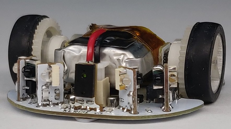
If you want to do something like [Carl Bujega]’s work on Designing Tiny Motors Right Into The Robot’s Circuit Board, you know you’re going to have to layout inductor coils directly on the board. SpiKi, a spiral inductor footprint generator for KiCad is what the Doctor prescribed.
This isn’t a comprehensive list by any means, so if you’re looking for a plugin we haven’t covered, then check out this roundup of plugins on the KiCad forum thread or this curated list on the xesscorp repository. If you come across one that isn’t listed, do let us know in the comments below.


 Recently, [Maurice] has released