Quantcast
Channel: KiCAD – Hackaday
Viewing all 169 articles
Browse latest View live

Git Your PCBs Online

$
0
0

Last time, I’ve shown you how to create a local Git repository around your PCB project. That alone provides you with local backups, helping you never lose the changes you make to your files, and always be able to review the history of your project as it developed.

However, an even more significant part of Git’s usefulness is the ability to upload our creations to one of the various online Git repository hosting services, and keep it up to date at all times with a single shell command. I’d like to show you how to upload your project to GitHub and GitLab, in particular!

Recap

First off, let’s recap what goes into creating a repository. Here’s a sequence of commands you can refer to – these commands have been explained in the last article, so they’re here in case you need a cheatsheet.

# setting up identity - these are public, and can be fake
git config --global user.name "John Doe"
git config --global user.email johndoe@example.com
# initializing a repository
git init .
git branch -M main
# before your first commit, you add your .gitignore file
# then, add files as needed - use 'git status' to check in
git add board.kicad_pcb
[...]
git add README.md
# or, given proper .gitignore, you can just do this:
git add .
# put your added changes into a commit
git commit
# an editor will open to write your commit message

What if you don’t happen to have a PCB project handy? Here’s a repository with a Jolly Wrencher SAO board that you can download it as a .zip archive through the GitHub interface. It’s already a repository – if you’d like to test these commands out but don’t yet have a PCB project handy, you can freely push this repository to your own GitHub or GitLab account as a test exercise! If you’d like to start anew and also practice the “repository creation” part, just delete the .git directory in the project root.

What’s The Difference?

Both GitHub and GitLab act as frontends for your repository. They also provide an extra place to dump your code – you could also just use a flash drive or a server with an SSH account. But hosting gives you a web interface where other people can take a look at your code and its README so they know if your code interests them, ask you questions, share their own code changes with you, download any extra related files (like gerbers) that you might’ve uploaded, and do a myriad of other useful things. You don’t need to use any of these features – you can disable all of them, but they’re there as soon as they might prove useful to you.

GitHub is the most well-known platform, and it’s been a trendsetter in many aspects. A major part of small-scale software and hardware hacking action happens on GitHub, and a lot of repositories you might find yourself interested in contributing to, will be there as well. There’s a lot of tutorials that work with GitHub, and fun tooling like this command-line GitHub UI we’ve covered.

GitLab is a less-known but no less useful platform that you can use for your code, PCBs and documents, and it has important advantages over GitHub. First and foremost, the GitLab software itself is fully open-source, so you can self-host it, and many do. It’s not the only self-hostable service, but it’s one of the most prominent and feature-complete ones. Just like with WordPress being both a software suite and a platform, you don’t have to self-host it. If you want somewhere to host your repositories on, you can go to gitlab.com and register an account, just like people do with GitHub.

There’s stars flying in the background of this signup form and each transition is flashy. Also, it took me 10 seconds to find where to enter my details on the signup page.

There’s a variety of frontends for online browser-accessible repository hosting – Gitea is another one that you will encounter every now and then and can easily self-host, and there’s a slew of other frontends that people have been using over the years. With knowledge of how two of these prominent frontends operate, what they have in common and how they differ, you will quickly find your way around any other frontend.

Registering on both websites is kinda similar. GitHub’s signup form is excessively flashy – it’s clear they invested quite a bit of money and effort into making it, but it’s not clear whether that was the right choice. Gitlab’s registration process is way calmer and generally more like what you’d expect out of a regular website. At certain points, both will ask you to confirm your email address – after doing that, your account will be ready to use.

Repository Creation

On both platforms, you’ll need to create a repository and register it with the platform first. You can’t just upload code to your account from the command line at a whim – the corresponding repository has to be created on the platform side before you can upload to it. There’s commandline tools to assist with the ‘creation’ step, thankfully!

Github’s and Gitlab’s processes are similar, each providing some quality of life features. On both, the “New Repository” button is quite apparent, and clicking it, you’re invited to input repository name – on GitHub, also an optional description. On GitLab, you’ll want to use the “Create blank project” option. The options to add a README, .gitignore and license can be useful. If you don’t have some of these in the repository, feel free to check these boxes or push those buttons; don’t check any of them if you’re using the Jolly Wrencher files as an exercise, unless you’re looking for a difficulty tweak in your Git learning journey.

If you’re just starting a software project, GitLab offers plenty of templates and integration options

Both GitHub and GitLab helpfully gives you a bunch of command-line instructions on how to proceed with uploading your local repository. Half of those instructions are about adding a very barebone README and making your first commit. Having a README in your PCB project folder is a good practice, though perhaps having an empty or a single-line one is a bit of a letdown to your repository viewers. If you don’t care about people looking at your repository, however, don’t worry about it.

The important lines are the git remote and git push ones, with git branch being helpful. These are where the upload magic happens. git remote is the command that you use to manage your, well, remote aka non-local Git mirrors for a given repository, and git push is the command that you use to send changes from your repository to a mirror. git branch -M main renames your primary branch to ‘main’ – most tutorials nowadays use ‘main’, which will make your life a bit easier.

A Short Authentication Detour

Before we can push, however, we need to sort out authentication – as in, how do we show the platform that the person executing this commandline is a person entitled to upload data to this repository. The two platforms achieve this in different ways. For GitHub, the usual login-plus-password combo won’t do – being a platform where people share code used by millions of people, mostly verbatim and without checks, they have tightened their defenses, and put more responsibility on our shoulders.

You have two routes when it comes to uploading to GitHub. Either you go the HTTPS route, and then you create a token that you use in place of your password. Alternatively, you go the SSH route, which means you generate and upload a public key you use for authentication. These are both secure options and they’re paramount if someone else depends on your code being malware-free. That said, one could argue they’re overkill for uploading a few PCBs. Both of these options are something you can do once and forget about, GitHub has short tutorials to help you set one of these methods up, and tools like GitHub Desktop or GitHub CLI take care of it for you.

GitLab, however, doesn’t mind letting you upload using the same password that you used to create your account. There’s security benefits to using keys instead of passwords – they’re not bruteforceable, they can be easily revoked, and compromising an SSH key doesn’t endanger your entire account. Plus, you can (and should) passphrase-protect your keys. There’s also undeniable comfort with only using a password – you don’t have to store a token or register an SSH key for every machine you want to work from.

SSH keys are nice. For “your own computer” use, they’re in many ways nicer than password authentication. If you’re on Linux, you get SSH keys for basically free, and I recommend you figure out how to use them – you likely already use your key to SSH into your friendly Raspberry Pi; same goes for MacOS. On Windows, there’s tutorials on how you can generate a SSH key that you can use with Git.

Finally, Uploading

Having sorted the authentication way out, you should be ready to upload your code. Let’s point your local Git repository configuration at the right place. You will tell Git that this local repository corresponds to a remote repository, colloquially referred to as a ‘remote’.

If you have one remote, it’s typically named ‘origin’ – that’s just a convention, you can name it whatever; you can have multiple remotes, but if you name it ‘origin’, tutorial compatibility will be better, again. Both GitHub and GitLab will give you the URL to use as a remote URL, depending on whether you picked HTTPS or SSH authentication – GitLab won’t give you SSH URLs until you upload a SSH key, whereas GitHub will happily give you the URLs but you won’t be able to use them.

Whichever you pick, run the command git remote add origin YOUR_URL, substituting YOUR_URL with the URL that you’re using, of course. This tells your Git repository where to upload, and now you’re one command away from from having your files mirrored online. In the beginning, that command will be git push -u origin main – for all subsequent pushes, it will just be as short as git push.

If you decided to add a README, a license file or a .gitignore file, you will actually want to do git pull before git push. This is because those files have been added by GitHub/GitLab as separate commits into your repository, and they don’t exist in your local repository yet, which means you have two repositories with diverging commit history. In this case, your repository will absorb the upstream changes and save them on top of your file.

Having made the first push into your repository, you can now open your GitHub/GitLab repository page in the browser and see your files uploaded there. Whenever you next make and commit your changes, syncing them to your computer is a single git push away.

A Few Reminders

If you push and then use commit --amend to fixup things, you will want to git push --force, since the last commit would’ve been amended, regenerating its hash and making it inconsistent with the last commit you just pushed into the remote repository. That said, doing force pushes is generally ill-advised, and you’re better off making an additional commit afterwards. This is mostly relevant if you’re working with others, because they might have pulled from your repository between you pushing the original commit and the amended one.

This is how a conflict looks. You can push --force, but typically a different solution is desired.

If you ever need to download your repository on a different computer, the command you can use is git clone with the URL after it. The “Download ZIP” option is viable, but you don’t always have a web UI handy – for instance, on headless installs, like a Raspberry Pi you might be setting up with some self-written or helpfully provided software.

For me personally, as I use the command line heavily, I find git clone to be a way faster option compared to ZIP download. If the repository is public, using the HTTPS URL for cloning it won’t need any authentication – in fact, on GitHub and GitLab, you can git clone the repository URL as you see it in your browser. Try out git clone https://github.com/CRImier/jolly_wrencher_sao for example.

Shared For Everyone To Learn From

Both GitHub and GitLab are good options for a hardware hacker looking to keep a few PCB projects online, and you can always spin up a private server if need be. The upload process can be a bit involved to set up, but once you’ve set it up, you’re three commands away from getting the most up-to-date version of your PCB design online and available to all interested. Next time, I’d like to show how two or more hackers can collaborate on PCB projects using Git!


Scripting Coils For PCB Motors

$
0
0

PCB inductors are a subject that has appeared here at Hackaday many times, perhaps most notably in the electromagnetic exploits of [Carl Bugeja]. But there is still much to be learned in the creation of the inductors themselves, and [atomic14] has recently been investigating their automatic creation through scripting.

A simple spiral trace is easy enough to create, but when for example creating a circular array of coils for an electric motor there’s a need for more complex shapes. Drawing a trapezoidal spiral is a surprisingly difficult task for a script, and we’re treated to a variety of algorithms in the path to achieving a usable design.

Having perfected the algorithm, how to bring it into KiCAD?  The PCB CAD package has its own Python environment built-in, but it’s not the most flexible in which to develop. The solution is to write a simple JSON interpreter in KiCAD, and leave the spiral generation to an external script that passes a JSON. This also leaves the possibility of using the same code in other PCB packages.

You can watch the whole video below the break. Meanwhile for more PCB electromagnetics, watch [Carl Bugeja]’s 2019 Supercon interview.

MikroLeo, A 4-Bit Retro Learning Platform

$
0
0

MikroLeo is a discrete TTL logic-based microcomputer intended for educational purposes created by [Edson Junior Acordi], an Electronics Professor at the Brazilian Federal Institute of Paraná, Brazil. The 4-bit CPU has a 
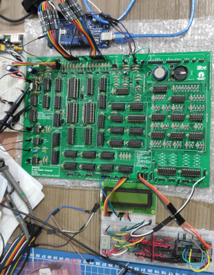
Harvard RISC architecture built entirely from 74HCT series logic mounted on a two-sided PCB using only through-hole parts. With 2K words of instruction RAM and 2K words of addressable RAM, the CPU has a similar resource level to comparable machines of old, giving students a feel for how to work within tight constraints.

Simulation of the circuit is possible with digital, with the dedicated PCB designed with KiCAD, so there should be enough there to get cracking with it. Four 4-bit IO ports make interfacing easy, with dedicated INput and OUTput instructions for the purpose. An assembler, compiler, and emulator are all being worked on (as far as we can tell) so keep an eye out for that, if this project is of interest to you.

We like computers a bit around these parts, the “hackier” and weirder the better. Even just in the 4-bit retro space, we’ve seen so many, from those built around ancient ALU chips to those built from discrete transistors and diodes, but you don’t need to go down that road, an emulation platform can scratch that retro itch, without the same level of pain.

Alpakka: A Creative Commons Game Controller

$
0
0

Input Labs’ mission is to produce open-source Creative Commons hardware and software for creating gaming controllers that can be adapted to anyone. Alpakka is their current take on a generic controller, looking similar to a modern Xbox or PlayStation controller but with quite a few differences. The 3D printed casing has a low-poly count, angular feel to it, but if you don’t like that you can tweak that in blender to just how you want it. Alpakka emulates a standard USB-attached keyboard, mouse, and Xinput gamepad in parallel so should just work out of the box for both Linux and Windows PC platforms. The firmware includes some built-in game profiles, which can be selected on the controller.

No special parts here, just 3D prints, a PCB and some nuts and bolts

The dual D-pads, augmented with an analog stick, is not an unusual arrangement, but what is a bit special is the inventive dual-gyro sensor arrangement –which when used in conjunction with a touch-sensitive pad — emulates a mouse input. Rest your thumb on the right-hand directional pad and the mouse moves, or else it stays fixed, kind of like lifting a mouse off the pad to re-center it.

The wired-only controller is based around a Raspberry Pi Pico, which has plenty of resources for this type of application giving a fast 250 Hz update rate. But to handle no fewer than nineteen button inputs, as well as a scroll wheel, directional switch, and that analog stick, the Pico doesn’t have enough I/O, needing a pair of NXP PCAL6416A I2C IO expanders to deal with it.

The PCB design is done with KiCAD, using a simple 3D printed stand to hold the PCB flat and the through-hole components in place while soldering. Other than a few QFN packages which might be a problem for some people, there is nothing tricky about hand-soldering this design.

We’ve been seeing custom game controllers as long as we’ve been hacking, here’s an interesting take on the mouse-integration theme. If you’re comfortable rolling the hardware side of things, but the firmware is a sticking point, then perhaps look no further than this neat RP2040 firmware project.

Thanks to [aamott] for the tip!

KiCad 2022 End-of-Year Recap and 7.0 Preview

$
0
0
KiCad 2022 Year End Recap

[Chris Gammell] moderated the KiCad 2022 End-of-Year Recap with several KiCad developers and librarians. They reviewed what’s been bubbling up in the nightly KiCad 6 builds, what we can expect from KiCad 7, and even answered some questions from the user community. Over the course of 2022, the KiCad project has grown both its development team and library team. The project even has a preliminary support commitment from the CERN Drawing Office!

Improvements to the KiCad Schematic Editor include smart wire dragging that simplifies moving components around within schematic diagrams. Components selected in the schematic now remain selected while switching to the PCB Editor. Internal documentation of schematics has advanced with support for fonts, embedded graphics, and the inclusion of hypertext links to datasheets and other reference materials. New features for PDF generation offer interactive files and links between sheets.

A new search panel within the KiCad PCB Editor supports finding components by footprint, net, or text search. A property panel allows common properties to be edited across multiple selected items. While a full-blown auto-router remains outside of the scope for KiCad, “push and shove” routing is faster and easier. An “attempt to finish” feature routes a quick connection for the currently selected trace, and “pack and move” positions all selected footprints into proximity to simplify placing them as neighbors within the board layout.

The KiCad PCB Editor also adds support for the use of fonts and inverted “knockout text” which even works on copper zones. Bitmap graphics can be imported and scaled beneath layout work as reference illustrations. Private footprint layers can be used to place extra documentation within footprints. The design rule checker (DRC) now can catch more layout issues, especially those that may impact manufacturability.

These are just a sampling of the impressive improvements we can expect with KiCad 7.0. There are also additions to circuit simulation and modeling features, a new command line interface for script-based automation, ARM64 support for KiCad running on Apple silicon, and a huge number of additions to the default library including symbols, footprints, and 3D Viewer models.

The KiCad team suggests several ways to support the project. There are always needs for additional developers and librarians. Financial contributions can be made at kicad.org. As users, we can run the nightly builds, try to break them, and give feedback in the form of detailed bug reports. Community testing will help make KiCad 7.0 as solid as possible. The project team is also seeking open hardware projects to include with KiCad 7.0 as demos.  For example, the StickHub project was included with KiCad 6.0 as a demo.

The official release of KiCad 7.0 is currently scheduled for January 31, 2023. While we wait, let’s flashback to our January 2022 presentation of what features made it into the KiCad 6.0 release.

KiCanvas Helps Teach And Share KiCad Projects In Browsers

$
0
0
Showing KiCanvas board viewer component inside a browser window, with a board being displayed and toggleable layers

KiCad is undeniably the hacker favourite when it comes to PCB design, and we’ve built a large amount of infrastructure around it – plugins, integrations, exporters, viewers, and much more. Now, [Stargirl Flowers] is working on what we could call a web viewer for KiCad files – though calling the KiCanvas project a “KiCad viewer” would be an understatement, given everything it aims to let you do. It will help you do exciting things like copy-pasting circuits between KiCad and browser windows, embed circuits into your blog and show component properties/part numbers interactively, and of course, it will work as a standalone online viewer for KiCad files!

Of course, the “board viewer” part of the project is exceptionally handy alone, and will let you quickly show your PCB designs to others without having KiCad installed. When it comes to schematics and PCB embed features, we can already see examples of KiCanvas in action, too – with exploreable circuits in the extensive writeup about a RP2040-based LumenPnP control board, and a PCB view in an assembly guide for a precision adder. Quite a few basic goals are already achieved and the project aims to become open-source in February, but there’s plenty to work on – mobile browser support, blog integrations, assembly helper features, and of course, an inevitable pile of testing and polish – for these, you can sponsor [Stargirl] on GitHub, for perks like early access to the project.

When sharing your projects with others, embedding a JPEG of your schematic only gets you so far, so given all the interactivity you can have, browsers and KiCad files are a match made in heaven. Projects like KiCanvas end up as building blocks that hackers can rely on – like the InteractiveHtmlBom project, which now helps quite a few projects provide assembly diagrams, or the Pinion project that lets you quickly create wiring diagrams for your PCB.

We thank [Ben Delarre], [Mithro] and [Helge Wurst] for sharing this with us!

Building a Fake Printer to Grab Screenshots Off the Parallel Port

$
0
0

[Tom Verbeure] recently found himself lamenting the need to take screen grabs from an Advantest R3273 spectrum analyzer with a phone camera, as the older gear requires you to either grab tables of data over an expensive GPIB interface card, or print them to paper. Then he realized, why not make a simple printer port add-on that looks like a printer, but sends the data over USB as a serial stream?

On the hardware side, the custom PCB (KiCAD project) is based on the Raspberry Pi Pico. Obvious form factor issues aside ([Tom] did revise the PCB to make it smaller) this is a shrewd move, as this is not a critical-path gadget so using the Pico as a USB-to-thing solution is a cost-effective way to get something working with minimal risk. One interesting design point was the use of the 74LVC161284 special function bus interface that handles the 5 V tolerance that the RP2040 lacks, whilst making the project compliant with IEEE-1284 — useful for the fussier instruments.

Using the service manual of the Sharp AP-PK11 copier/printer as a reference, [Tom] again, shows how to correctly use the chip, minimizing the design effort and scope for error. The complete project, with preliminary firmware and everything needed to build this thing, can be found on the project GitHub page. [Tom] does add a warning however that this project is still being worked on so adopters might wish to bear that in mind.

If you don’t own such fancy bench instrumentation, but grabbing screenshots from devices that don’t normally support it, is more your thing, then how about a tool to grab Game Boy screenshots?

Create Your RTL Simulations With KiCAD

$
0
0

[Bob Alexander] is in the process of designing a homebrew discrete TTL CPU, and wanted a way to enter schematics for digital simulations via a Verilog RTL flow. Since KiCAD is pretty good at handling hierarchical schematics, why not use that? [Bob] created a KiCAD plugin, KiCadVerilog allowing one to instantiate and wire up the circuits under consideration, and then throw the resulting Verilog file at your logic simulator of choice.

KiCadVerilog doesn’t do all the hard work though, as it only provides the structure and the wiring of the circuit. The actual guts of each TTL instance needs to be provided, and a reference to it is manually added to the schematic object fields. That’s a one-time deal, as you can re-use the component library once generated. Since TTL logic has been around for a little while, locating a suitable Verilog library for this is easy. Here’s ice-chips-verilog by [TimRudy] on GitHub for starters. It’s intended as a collection for Icestudio (which is also worth a look). Still, the Verilog code for many TTL series devices is presented ready for the taking, complete with individual test benches in case you need them.

Check out the project GitHub page for the module source code, and some more documentation about the design process.

We’ve seen many RTL hacks over the years, here’s an interesting way to generate a PCB layout with discrete logic, direct from the RTL.


KiCad 7.0.0 Is Here, Brings Trove Of Improvements

$
0
0
Screenshot of KiCad 7 feature that lets you overlay a PCB bitmap image and draw traces over it, being used for board reverse-engineering purposes

Yesterday, the KiCad team has released KiCad 7.0.0 – a surprise for those of us who have only gotten used to the wonders of KiCad 6, and it’s undoubtedly a welcome one! Some of these features, you might’ve seen mentioned in the KiCad 2022 end-of-year recap, and now, we get to play with them in a more stable configuration. There’s a trove of features and fixes for all levels of KiCad users, beginners, hobbyists and professionals alike – let’s start with some that everyone can appreciate!

First thing you’ll want to hear about is the kicad-cli binary – yes, KiCad is getting native commandline support, and you can get a dozen different things out of it, from gerbers and BOM files, to STEP and schematic PDFs. Previously, it’s always been that moving from schematic to PCB layout would have you end up in the middle of a not-yet-positioned footprint ocean – now, KiCad 7 gives you tools to automate placement of newly added footprints! There are routing features that automate trace drawing – it’s not autorouting exactly, but it brings quite a few features of a simple yet powerful autorouter to your fingertips. Last but not least, if you ever had KiCad mysteriously crash on you and you were to busy to do a bug report, you’ll be glad to hear that KiCad now has privacy-conscious crash reporting for debugging crashes like these – an addition that has already helped figure out a few long-standing KiCad crash-inducing bugs.

A schematic screenshot showing a greyed out component marked as "do not populate"
A greyed out Do Not Populate component

For those of us taking KiCad work beyond beginner level, there’s a solid array of additions, too! Drag&drop stands out the most, perhaps – it lets you append schematic and PCB portions into your boards from other projects, and if doesn’t signify sub-design support already, then it’s definitely a step in the right direction! Then, there’s features like database integration support for component information field population, Do Not Populate indications that grey out the schematic symbol and remove the component from BOM and place files, simulator integration improvements, hyperlinks in schematics that are even preserved when exporting to PDF, mechanical and design rule check improvements, automatic zone refilling, and a dozen more cool things. We especially like the feature pictured above, that lets you reverse-engineer boards by placing a bitmap image of the board in question inside the PCB editor working field, drawing tracks on top of it, even with support for side flipping – check out the release blog post for a video demonstration!

This release is seriously exciting, and it would seem like the KiCad team is moving towards a faster major release schedule, comparing today’s date with KiCad 5 release in December 2018 and KiCad 6 release in December 2021. We can’t wait for the trove of bugfixes that inevitably follow a .0.0 release like this, however, on a larger scale, it seems like we might see features get from testing to stable releases quicker, and that’s a large benefit for keeping KiCad the highly competitive PCB suite that it is. Some of us have already been daily-driving this KiCad version in its ‘nightly’ state, and we can’t wait see these features applied in hackers’ projects!

Physics-Controlled Component Auto-Placer

$
0
0

[Jarrett] recently stumbled upon a class of drawing algorithms called force-directed graphs, which artificially apply forces to the elements. The final graph is then generated by applying the laws of physics and letting the system reach equilibrium. This can often result in a pleasing presentation of things like mind maps and other diagrams without having to hand-place everything. He realized that this approach almost mimics the way he places components when doing a PCB layout. Out of curiosity or intense boredom, we’re not sure which, he decided to implement this in a tool that interacts with KiCad ( see animated GIF below the break ).

He has to ignore certain nets such as power and ground rails, because they distort the result. This simulation treats the nets as springs, and the center of each footprint behaves a charged particle. [Jarrett] added a twist, literally, to the usual implementations — each net pulls on its pin, not the part center, and therefore the chips will both rotate and be pushed around as the system stabilizes.

The results are sometimes quite striking. Useful? Dubious, but maybe!

The project code is up on GitHub, but is very experimental and he is unlikely to carry it further. Among the missing features, the Python code must be tweaked for each different netlist files and other parameters, and there is no way to feed the result back into KiCad. But this is enough for [Jarrett], who only set out to see if the concept was possible. The code is available if anyone wants to try their hand at taking this to the next level.


Kicad Autorouting Made Easy

$
0
0

One of the most laborious tasks in PCB layout is the routing. Autorouting isn’t always perfect, but it is nice to have the option, even if you only use it to get started and then hand-tune the resulting board. Unfortunately, recent versions of Kicad have dropped support for autorouting. You can, however, still use Freerouting and the video from [Mr. T] below shows you how to get started.

There are three ways to get the autorouting support. You can install Java and a plugin, you can isntall using a ZIP file, or you can simply export a Specctra DSN file and use Freerouting as a standalone program. Then you import the output DSN file, and you are done.

Not only does [Mr. T] show you how to do a simple USB board, he also shows you how to rip up the autorouter’s work if you don’t like it. He also covers some tips to get the best results with the router.

For example, it is often advantageous to manually layout a few critical tracks before you run the autorouter. You can also use net classes to specify parameters for some tracks.

Overall, this is a worthwhile thing to do. After all, you don’t have to use autorouting, but it is nice to have it available if you want it. If you don’t like Freerouting, you can try a different solution. Of course, these routers use DSN, so you can use them with many different tools if you aren’t using Kicad.

Hackaday Links: April 16, 2023

$
0
0
Hackaday Links Column Banner

The dystopian future you’ve been expecting is here now, at least if you live in New York City, which unveiled a trio of technology solutions to the city’s crime woes this week. Surprisingly, the least terrifying one is “DigiDog,” which seems to be more or less an off-the-shelf Spot robot from Boston Dynamics. DigiDog’s job is to de-escalate hostage negotiation situations, and unarmed though it may be, we suspect that the mission will fail spectacularly if either the hostage or hostage-taker has seen Black Mirror. Also likely to terrify the public is the totally-not-a-Dalek-looking K5 Autonomous Security Robot, which is apparently already wandering around Times Square using AI and other buzzwords to snitch on people. And finally, there’s StarChase, which is based on an AR-15 lower receiver and shoots GPS trackers that stick to cars so they can be tracked remotely. We’re not sure about that last one either; besides the fact that it looks like a grenade launcher, the GPS tracker isn’t exactly covert. Plus it’s only attached with adhesive, so it seems easy enough to pop it off the target vehicle and throw it in a sewer, or even attach it to another car.

Have you ever wondered how Uber sets its prices? We haven’t, because we’ve never used a ridesharing service, but apparently, some reporters in Belgium with that very question did an informal experiment and found that it may have something to do with the battery charge level on your phone. They used two different smartphones to hail a ride from their office to the center of Brussels. The phone with 84% charge got a price of €16.60, while the phone with only 12% remaining was quoted €15.56. The experiment has obvious flaws, like an n of 1 and the fact that they used two different phones rather than the same phone at different charge states. And Uber denies that they take battery charge into account when determining a ride price. But we have to admit it seems like using battery state as a proxy for user desperation seems pretty smart, so we’d like to see more work done on this.

In more dystopic news, the mayor of an Australian city may become the first person to sue ChatGPT for defamation. Brian Hood, newly elected mayor of the enchantingly named Hepburn Shire, discovered that constituents were being told by the chatbot that he had been embroiled in a foreign bribery scandal in the early 2000s and naming him the guilty party. The first part was true, insofar as he was the whistleblower in the cases, and was never charged with anything. His lawyers have sent a takedown notice to OpenAI but haven’t heard back, so there may be a precedent-setting lawsuit in the offing.

Sad news for anyone who cut their engineering teeth on Meccano as the last factory dedicated to making the construction toy is getting ready to close its doors. The Calais plant, which has been making Meccano for more than 40 years, is being closed in 2024 due to — what else — supply chain issues and the rising cost of materials. While the plant closure will impact the 51 people who work there, it’s not the end of the line for the Meccano brand, since the toy will continue to be made under contract by factories in Europe, Asia, and Latin America. But it is sad to see the decline of a brand like this, especially when it helped launch so many engineering careers.

Ever wish there was a Google Earth for Mars? We’ve got you covered.

And finally, if you’re looking for a quick way to get up to speed on KiCad 7, you could do worse than this 13-minute introductory video. It’s not exactly for EDA beginners, but if you’re coming over from Eagle or some other platform and have the basic vocabulary, these five steps will get you going. Sadly, though, you still won’t know for sure how to pronounce “KiCad” after the video.

Importing EAGLE Projects Into KiCad 7, And How To Fix Them

$
0
0

Migrating a PCB design from one CAD software package to another is no one’s favorite task. It almost never works cleanly. Often there are missing schematic symbols, scrambled PCB footprints, and plenty of other problems. Thankfully [shabaz] shows how to import EAGLE projects into KiCad 7 and fix the most common problems one is likely to encounter in the process. Frankly, the information couldn’t come at a better time.

This is very timely now that EAGLE has gone the way of the dodo. CadSoft EAGLE used to be a big shot when it came to PCB design for small organizations or individual designers, but six years after being purchased by Autodesk they are no more. KiCad 7 is a staggeringly capable open-source software package containing some fantastic features for beginner and advanced designers alike.

Of course, these kinds of tutorials tend to be perishable because software changes over time. So if you’re staring down a migration from EAGLE to KiCad and could use some guidance, there’s no better time than the present. [shabaz]’s video showing the process is embedded below.

Thanks to [problemchild68] for the tip!

Nail, Meet KiCad

$
0
0

You know the old saying. When all you have open is KiCad, everything looks like a PCB. That was certainly true for [Evan], who needed to replace a small part recently and turned to PCBs to get the job done.

The part in question was a sheered apart detent cam from a retractable cord reel. Glue and epoxy might have worked, and [Evan] was worried about how a 3D printed PLA part would have held up. The part is an extruded 2D shape, making PCBs a non-traditional but viable choice. Using the old scanner trick, he traced the outline in KiCad 7 (which adds image references). Then with the five boards stacked up, solid core wire, solder, and a propane torch worth of heat fused it. Ultimately, this machine’s tolerances are generous, so it worked wonderfully.

Was it the “right” tool for the job? Right or wrong, it is hard to argue that in terms of durability and ease per dollar, this doesn’t come out on top. PCB files are on GitHub if you have a 5020TF-4c retractable cord reel that needs a new cam. PCBs have a fun way of adopting different use cases like enclosures, but perhaps the idea of PCBs as a mechanical part could be applied elsewhere.

Easyeda2KiCad: Never Draw a Footprint Again

$
0
0

What if I told you that you might never need to draw a new footprint again? Such is my friend’s impression of the tool that she’s shown me and I’m about to show you in turn, having used this tool for a few projects, I can’t really disagree!

We all know of the JLCPCB/LCSC/EasyEDA trio, and their integration makes a lot of sense. You’re expected to design your boards in EasyEDA, order the components on LCSC, and get the boards made by JLCPCB. It’s meant to be a one-stop shop, and as you might expect, there’s tight integration between all three. If there wasn’t, you’d be tempted to step outside of the ecosystem, after all.

But like many in this community, I use KiCad, and I don’t expect to move to a different PCB design suite — especially not a cloud one. Still, I enjoy using the JLCPCB and LCSC combination in the hobby PCB market as it stands now, and despite my KiCad affinity, it appears that EasyEDA can help me after all!

All Data, No Hassle

One of the hard-to-beat EasyEDA-LCSC integration aspects is that you can easily add LCSC parts to your boards. There’s no need to hunt for footprints and symbols, they’re all ready to go. You simply get the LCSC inventory at your fingertips, or at least the part of it that’s been documented by EasyEDA engineers. Indeed, this information isn’t just EasyEDA-specific, you can access it externally, and there’s a tool called easyeda2kicad that lets you download all the part files in KiCad format!

In the end, it fit with space to spare!

For instance, I was recently looking for microSD sockets — something that I have a tried and true part for. There’s a few hundred pieces in a bag next to my desk, even. Today’s constraint? It has to be less wide than the card itself, since I have to fit it into a narrow spot. Mouser didn’t have any good parts for me, but LCSC did. The sockets I found were also way cheaper, even including shipping and VAT. So, I’ve found a good part, but oh no, the footprint has ten pads and the mechanical dimensions are only half-intelligible, and I just want to get to drawing the long overdue board already!

All you need from here is the easyeda2kicad script installed – it takes the LCSC part number and creates the symbol, footprint and 3D model files for you automatically. To be clear, not all LCSC parts have been digitized. But that said, for one project of hers, my friend could successfully download a whole MXM slot, DisplayPort, miniDisplayPort and VGA connectors, and a few inductors with non-standard footprints; a combination that would typically need you to sit down in front of a PCB editor for a few hours, and that’s certainly not including the 3D models.

Limited, But Great Nevertheless

Choice in EDA software is something way less malleable than component and PCB service choice, and it rocks that this software now gives us an extra option. I’ve gone through a few projects by now with this script at the ready, the footprints and symbols have all worked as advertised, and while I still need to design footprints every now and then, they’re usually something exotic.

You could draw this from scratch, or you could run a script – the choice is yours

easyeda2kicad will absolutely help if, like me, you have a foot strongly in the JLCPCB+LCSC field. Or the Eastern parts field at all. I’ve given a good few thousand dollars to these two companies, for personal and business purposes alike, and I don’t see a reason I’d stop just yet. I’m not here to promote any specific company, of course, and you’ll guess correctly that I’ve had these footprints and symbols work for Aliexpress parts, too, as long as you find which LCSC part they correspond to.

There are, of course, a few problems. The footprints have dubious legal status — any license granted likely doesn’t include such external use, and while we wouldn’t foresee problems adding such parts to open-source projects, it’s a technicality to keep in mind. These symbols and footprints are untested unless we know otherwise, unlike parts in the KiCad library, and as usual, they might deviate from datasheet in important ways.

You’re also at the mercy of the EasyEDA API, which you might remember [Jan Mrazek]’s irreplaceable LCSC search tool had problems with in the past. The problems have since been resolved, but the situation has left a bad aftertaste.

You might think that this is free symbol and footprint galore, and in a way, it is! Of course, the LCSC-JLCPCB-EasyEDA trio still wins — you’re more likely to use their services if you use this tool. There’s a reason why Western manufacturers often provide the same services, giving you footprints, symbols and 3D models so that you have it easier starting a new design within their ecosystem. SnapEDA, a similar service for Western parts, has been a mainstay in the electronics world, and to think of it, it’s long overdue to have such an option for Eastern parts!


Hackaday Prize 2023: Circuit Scout Lends a Hand (Or Two) for Troubleshooting

$
0
0

Troubleshooting a circuit is easy, right? All you need is a couple of hands to hold the probes, another hand to twiddle the knobs, a pair of eyes to look at the schematic, another pair to look at the circuit board, and, for fancy work, X-ray vision to see through the board so you know what pads to probe. It’s child’s play!

In the real world, most of us don’t have all the extra parts needed to do the job right, which is where something like CircuitScout would come in mighty handy. [Fangzheng Liu] and [Thomas Juldo]’s design is a little like a small pick-and-place machine, except that instead of placing components, the dual gantries place probes on whatever test points you need to look at. The stepper-controlled gantries move independently over a fixture to hold the PCB in a known position so that the servo-controlled Z-axes can drive the probes down to the right place on the board.

As cool as the hardware is, the real treat is the software. A web-based GUI parses the PCB’s KiCAD files, allowing you to pick a test point on the schematic and have the machine move a probe to the right spot on the board. The video below shows CircuitScout moving probes from a Saleae logic analyzer around, which lets you both control the test setup and see the results without ever looking away from the screen.

CircuitScout seems like a brilliant idea that has a lot of potential both for ad hoc troubleshooting and for more formal production testing. It’s just exactly what we’re looking for in an entry for the Gearing Up round of the 2023 Hackaday Prize.

Where Did Your PCB Go Wrong? KiRI knows

$
0
0

When working on a PCB design in KiCad, it’s helpful that the files are all text and can easily be checked into Git or other source control. However, stepping back through the revisions to determine where precisely a trace got routed wrong can be tricky. [Leandro] started with a simple script that exported the KiCad project to an image for inspection — over time it grew into a full-blown visual diff tool named KiCad Revision Inspector (KiRI).

The primary mechanism exports the revisions of a KiCad 5, 6, or 7 project to SVG, which can then be compared via a handy onion skin view. As this is a tool written for those using KiCad, shortcuts are a huge part of the experience. A command line interface generates artifacts to view the diff in any web browser. As these outputs have the KiRI tooling baked in, it is relatively easy to archive the output as a build artifact and allow easy access to review design changes.

For the long-time reader, you might remember back in 2018 talked about another diffing tool called plotgitsch (which this KiRI uses for KiCad 5 projects). KiCad has grown significantly in the last five years. It might be time to update our tips to utilize Git better for your PCB designs.

Thanks to [Marcel] for sending this one in.

Hackaday Prize 2023: Jumperless, The Jumperless Jumperboard

$
0
0

Jumperless is a jumperless breadboard with multicolored LED visualization of signals in real-time. Sounds like magic? This beautifully executed entry to the 2023 Hackaday Prize by [Kevin Santo Cappuccio] uses a boatload of CH446Q analog switch ICs to perform the interconnect between the Raspberry Pi Pico header and the jumper board (or breadboard if you prefer.)

This will add some significant resistance, but for low currents and digital logic levels, this should not be a major concern. Additionally, there are two DAC channels and four ADC channels to help break out of the digital 
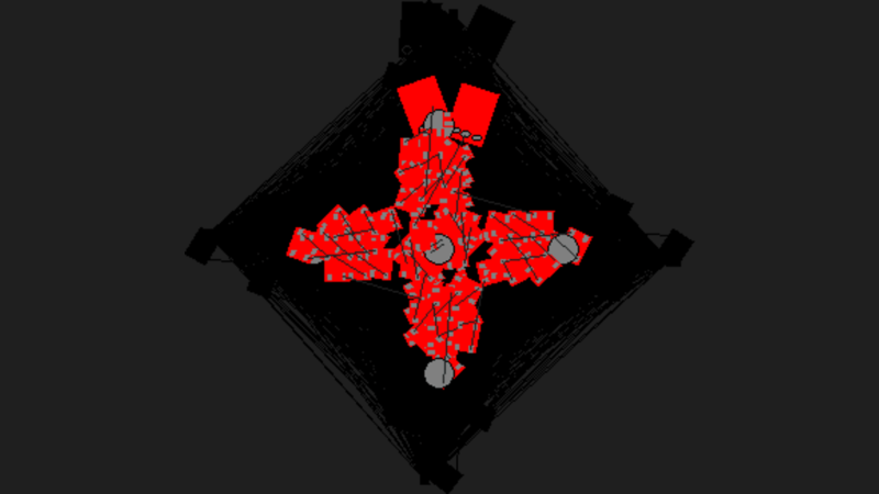
world, which could make for some very interesting non-trivial applications.

The visualization of the Pico header signals is solved neatly with a tiny wishbone-shaped PCB that is reverse-mounted to the back of the main board to illuminate upwards. The masking of the labels is done by using copper to mask off the individual signals and solder mask to draw in the legends. This PCB-level hacking is simply wonderful to see. The PCBs are designed with KiCAD, the design files for which you can find here. It appears however that [Kevin] needed to have the spring clips for the jumper board custom-made, so you’d need to contact them if you needed to get some for a build.

On the software side of things, [Kevin] currently recommends using Wokwi, to run the Arduino stack applications and to perform the signal routing to the virtual jumper board. You can follow how it works internally here. A Python-based bridge application runs on the host computer, which takes care of programming the interconnects as they are constructed, which looking at the demo in the embedded video, appears to ‘just work.’

One word of caution though — the bridge app uses Python requests and Beautiful Soup to scrape the Wowki project page, which could potentially make it vulnerable to getting out-of-sync with updates, so hopefully [Kevin] will keep track of this and keep them in sync.

Need some breadboarding tips? We got you covered. Talking of bread, here’s an 8-bit TTL breadboard-based CPU in a breadbin.

Thin Keyboard Fits in Steam Deck Case

$
0
0

Although some of the first Android-powered smartphones had them and Blackberries were famous for them, physical keyboards on portable electronics like that quickly became a thing of the past. Presumably the cost to manufacture is too high and the margins too low regardless of consumer demand. Whatever the reason, if you want a small keyboard for your portable devices you’ll likely need to make one yourself like [Kārlis] did for the Steam Deck.

Unlike a more familiar mechanical keyboard build which prioritizes the feel and sound of the keyboard experience, this one sacrifices nearly every other design consideration in order to be thin enough to fit in the Steam Deck case. The PCB is designed to be flexible using copper tape cut to size with a vinyl cutter with all the traces running to a Raspberry Pi Pico which hosts the firmware and plugs into the Steam Deck’s USB port. The files for the PCB are available in KiCad and can be exported as SVG files for cutting.

In the end, [Kārlis] has a functioning keyboard that’s even a little more robust than was initially expected and which does fit alongside the Deck in its case. On the other hand, [Kārlis] describes the typing experience as “awful” due to its extreme thinness, but either way we applaud the amount of effort that went in to building a keyboard with this form factor. The Steam Deck itself is a platform which lends itself to all kinds of modifications as well, from the control sticks to the operating systems, and Valve will even show you how.

Chip Shortage Engineering: Misusing DIP Packages

$
0
0

After years of seeing people showing off and trading their badge Simple Add-Ons (SAOs) at Supercon, this year I finally decided to make one myself. Now for a first attempt, it would have been enough to come up with some cool PCB art and stick a few LEDs on it. But naturally I started with a concept that was far more ambitious than necessary, and before long, had convinced myself that the only way to do the thing justice was to have an onboard microcontroller.

My first thought was to go with the venerable ATtiny85, and since I already had a considerable stock of the classic eight-pin DIP MCUs on hand, that’s what I started prototyping with. After I had something working on the breadboard, the plan was to switch over to the SOIC-8 version of the chip which would be far more appropriate for something as small as an SAO.

Unfortunately, that’s where things got tricky. I quickly found that none of the major players actually had the SMD version of the chip in stock. Both DigiKey and Mouser said they didn’t expect to get more in until early 2024, and while Arrow briefly showed around 3,000 on hand, they were all gone by the time I checked back. But that was only half the problem — even if they had them, $1.50 a piece seems a hell of a lot of money for an 8-bit MCU with 8K of flash in 2023.

The whole thing was made all the more frustrating by the pile of DIP8 ATtiny85s sitting on the bench, mocking me. Under normal circumstances, using them in an SAO wouldn’t really be a problem, but eight hand-soldered leads popping through the front artwork would screw up the look I had in mind.

While brooding over the situation my eyes happened to fall on one of the chips I had been fiddling with, it’s legs badly bent from repeated trips through the programmer. Suddenly it occurred to me that maybe there was a way to use the parts I already had…

In Case of Shortage, Bend Pins

The idea was simple enough; I’d program the ATtiny85, carefully bend its legs outward, and then push the chip down firmly onto an ESD mat to get it as flat as possible. From there, I could snip the legs off with a side cutter, but I thought limiting the interaction between the chip and metal tools was probably for the best. As such, the result is a chip that’s flat to the PCB like an SMD component, but with leads that extend much farther out than any traditional package.

Obviously, the body of a DIP chip is still much larger than its SOIC counterpart. But it’s not like I’m trying to build a smartphone here, a small bump on the back of the SAO is unlikely to bother anyone so long as it doesn’t physically collide with the badge it’s getting plugged into.

But of course, a bent chip is only half of the equation. To put this into practice on more than a one-off basis, you’d need a suitable footprint so compatible PCBs could be spun up.

A Word on Footprints

If you only ever used jellybean components in your PCB designs, you could probably go for quite some time before having to design your own footprint. But eventually, it’s going to catch up with you. As the complexity of your projects increases, you’ll inevitably run into a part that doesn’t have a digital representation in your electronic design automation (EDA) tool of choice.

With that in mind, creating custom footprints is a good thing to become familiar with ahead of time — nobody wants to have a project hung up as they struggle to get up to speed with a tool they never used before.

We’ve previously looked at automated tools that will pull footprints from online repositories and convert them into something KiCad will understand. This is a great capability to have, but it’s not infallible, and there’s always a chance you’ll run across some oddball component out there that doesn’t have a publicly available footprint; so there’s still value in learning how to do it manually.

As this is a pretty simple footprint, it’s a great example to get started with. Even if you don’t plan on smushing your old DIP8 chips into service as makeshift SMD components, I’d invite you to follow along here if you’ve never used KiCad’s footprint editor. While not presented as a step-by-step guide, it should at least help you wrap your mind around the workflow.

Running the Numbers

Under normal circumstances, the first step in making a footprint would be to consult the datasheet for the part in question. There, you’ll almost certainly find a diagram that describes in precise detail the geometry of the component. Assuming the datasheet is accurate and you don’t flub any of the figures, you should be able to make a footprint without ever having actually seen the physical part itself.

In this case though, our footprint doesn’t correspond with any proper package. With no handy diagram to follow, we’ll need to take some manual measurements before all is said and done. But it did start as a normal package, so the ATtiny85’s datasheet still provides some valuable clues.

The main thing we’re looking for here is the size and spacing of the leads. This is labeled as “e” in the diagram, which corresponds to 0.100 inches, or 2.54 mm. BSC means “Basic Spacing Between Centers”, which indicates the measurement refers to the center point of each lead and not the outside edges.

As the leads have a stepped shape, there’s two figures given for each one: “b” for the thin tip, and “b2” for the wider base. We’re after “b” in this case, which the chart says could be anywhere between 0.014 and 0.022 inches. Helpfully, it also gives us a nominal value of 0.018 inches (0.45 mm). We can also see that “L” shows the nominal length of each lead, not counting the base, to be 0.130 inches (3.3 mm).

Given the length of the leads and the width of the plastic package, we could come up with a good estimate of the “wingspan” for our flattened chip, but it was just as easy to grab the calipers and check the real-world dimensions:

So where does that leave us? First of all, we ain’t going to space with this thing, so we can round off some of those numbers. This can buy a little of wiggle room, since the parts will be hand soldered, and just makes it a bit easier to wrap your head around. Second, let’s stop mixing units and just stick with metric since that’s what the board house is going to want anyway.

The end result: a footprint that has eight pads of approximately 3 x 1.5 mm, spaced 2.54 mm from each other, with a span of around 16 mm.

Putting Your Foot Down

The KiCad Foorprint Editor tool works more or less the same as the PCB Editor, and shares many of the same tools and icons. So if you’ve already got a couple custom PCBs under your belt, wrangling the interface shouldn’t provide much of a challenge.

Once you’ve created a custom library (which can be per-project, or global for all of your projects) and named your new footprint, you’re given a blank canvas on which to drop your pads using the appropriately named “Add a Pad” tool. After placing the first pad you can edit its parameters to give it the desired dimensions, and from then on, any new pads you place will have the same size and shape. The pad number will also automatically increment, though its up to you to make sure they match the part’s actual numbering scheme.

Using the various measuring tools at your disposal, getting the pad spacing where you want it is pretty simple. The most important thing to remember here is probably to set a reasonable grid size so you don’t have pads snapping to weird positions. For this example a grid size of 0.5 mm would be fine, but for finer pitched components you’d want to drop that down.

Once the footprint looked about right, I used the Print command to run off a 1:1 duplicate on a piece of paper and checked that the ATtiny85 physically lined up with what would be copper pads on a real PCB.

Lessons Learned

Now, I’m not claiming to be the first person to come up with this idea. Indeed, our illustrious Editor in Chief Elliot Williams says this wasn’t an uncommon practice back when hobbyists started dipping their toes irons into the world of SMD. So this is less breaking new ground, and more blowing the dust off a technique that’s been lost to time.

Was it worth the effort? As you can see from the image at the right, I did get PCBs made with this custom footprint, and I had no problem soldering these previously through-hole components as if they were supersized SMD chips. But ultimately, even the cost of the DIP8 version came out to be more than expected.

As of this writing, Digikey wants $1.66 each for the ATTINY85-20U. So while I did assemble several of the SAOs using this technique, in the end I switched over to the newer tinyAVR 2 family of chips. They don’t come in eight-pin flavors anymore, but the extra flash, UPDI programming, and lower cost more than make up for a little extra soldering.

So while it wasn’t quite the solution I was hoping for, it was certainly a successful hack and a good chance to brush up on some valuable skills. As any reader of Hackaday knows — the journey can sometimes end up being more interesting than the destination.

Viewing all 169 articles
Browse latest View live


Latest Images

<script src="https://jsc.adskeeper.com/r/s/rssing.com.1596347.js" async> </script>